Skip to content
Akrivis Components and Tools
Menu
  • Home
  • Products
    • Cleaning & Contamination Control
      • Microelectronics Cleaning
        • NanoVapor
        • Vapor SUI 2
        • Vapor SUI Mini 2
        • Vapor SUI Mini 3 (Co-Solvent)
        • Vapor SUI Inline 2
      • SMT Cleaning
        • Hydro-clean AS
        • Hydro-clean MAX
        • Hydro-clean LRS
        • Hydro-clean LDS
        • Hydro-clean LDS-S
        • Hydro-clean LTS
        • Hydro-clean ARRAY
      • DI Water Generation
        • LDSJ-250L-CS
    • Lead Forming
      • Automatic Forming
        • APFL
      • Pneumatic Forming
        • PFL-FM (Fixed Mold)
        • PFL/BOTTOM
        • PFL/DPAK
        • PFL/OMEGA
        • PFL-1F
        • PFL-1M
      • SAPFL (Semi-Automatic)
      • Lead Cutting
        • DIP Cutter
        • FR CUT
        • PCL
        • PCL-Plus
      • Reconditioning
        • LRS-1
      • Through-Hole
        • THTF
    • Wire Bonding
      • M60W
      • PW22
    • Tinning
      • Super Tinning
      • Hyper Tinning
    • Thermal Processing
      • VTP2000
      • Heating Plate
      • Split-Type
      • Integrated Heating Stage
    • Spot Welding
      • SMSW II
    • Parylene Coating
  • About
  • News
  • Contact

Category: Latest News

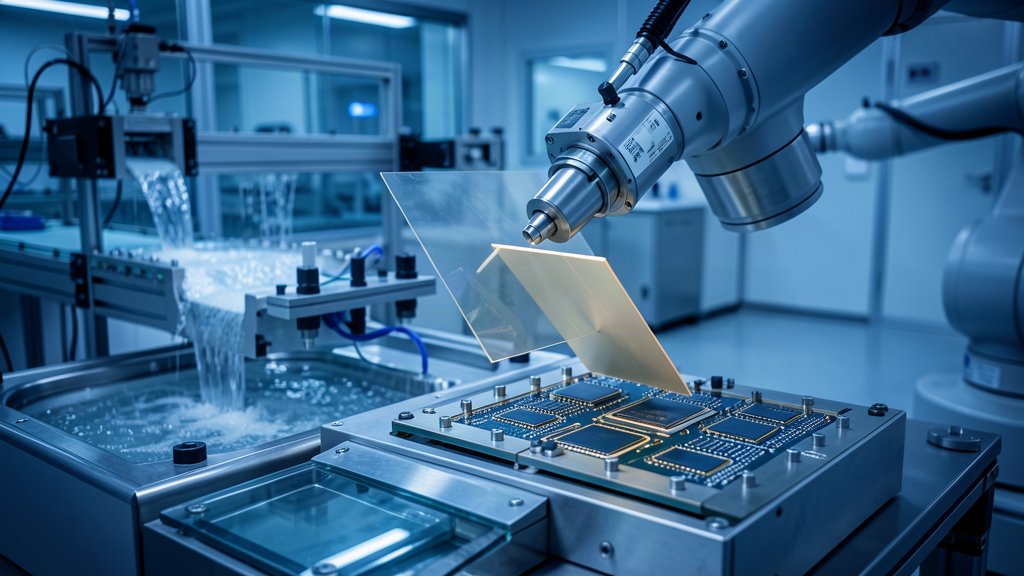
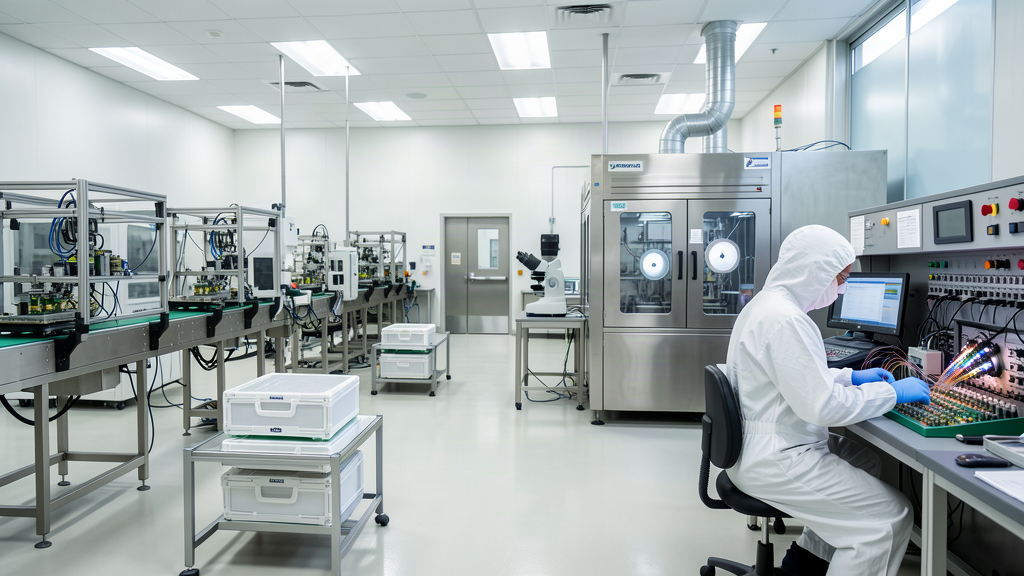
Semiconductor manufacturing cleanroom with precision PCB assembly equipment
Blog / Latest News

Section 232 Semiconductor Tariffs: What Domestic Manufacturers Actually Need to Build

In January 2026, the Trump administration imposed a 25 percent ad valorem tariff on certain advanced computing semiconductors under Section 232 of the Trade Expansion Act, citing the finding that …

Blog / Latest News

Micron $250B, TSMC $265B, and the Process Capability Gap Behind Made in America Semiconductors

Micron commits $250B and TSMC expands to $265B in U.S. semiconductor investment — but Made in America requires downstream process capability: contamination control, advanced packaging, legacy reconditioning, and full BOM traceability.

Blog / Latest News

TSMC’s $265B Arizona Bet and the Domestic Packaging Gap: What Electronics Manufacturers Actually Need to Build

TSMC’s $265B Arizona investment is the largest foreign direct investment in U.S. history — but building fabs is only the visible part. The harder challenge is assembling the domestic process ecosystem that makes those fabs productive.

Blog / Latest News

New Defense Supply Chain Executive Order Demands Domestic Process Capability — Not Just a “Made in America” Label

Executive Order 14415 requires defense contractors to trace every component and material back to its raw-material origin. For electronics manufacturers, that means real domestic process capability — not just a procurement checkbox.

Blog / Latest News

Semiconductor Tariffs, FAR Procurement Bans, and the NDAA: What Domestic Electronics Manufacturers Need to Know in 2026

Federal semiconductor tariffs, a new FAR rule banning covered semiconductors, and the FY2026 NDAA’s domestic sourcing deadlines are reshaping electronics manufacturing procurement. Here’s what process engineers and supply-chain teams need to know — and why domestic process capability matters more than labels.

Blog / Latest News

NVIDIA’s First ‘Made in America’ GPUs Ship to Taiwan for Packaging — Why Domestic Process Capability Still Matters

On July 27, 2026, NVIDIA and TSMC hit what WCCFTech reported as a milestone for U.S. semiconductor manufacturing: the first NVIDIA GB300 AI GPUs fabricated on TSMC’s 4nm node rolled …

Blog / Latest News

Made in America Means More Than a Label: Cleaning, Contamination Control, and the Domestic Semiconductor Process Gap

In early July, SEMI convened its annual Surface Preparation & Cleaning Conference (SPCC 2026) in Chandler, Arizona — the premier technical forum dedicated to advancing surface preparation, cleaning technologies, and …

Blog / Latest News

TTM Opens $130M Ultra-HDI PCB Facility: What Domestic Defense Electronics Manufacturing Really Requires

TTM Technologies opened a $130M Ultra-HDI PCB facility in Syracuse, NY with $30M from the Department of War. The facility highlights a critical reality: building domestic defense electronics requires more than capital equipment—it demands a full process ecosystem for contamination control, component preparation, and assembly.

Blog / Latest News

Stencil Cleaning vs. PCBA Cleaning: Different Problems, Different Solutions

Stencil Cleaning vs. PCBA Cleaning: Different Problems, Different Solutions In a standard SMT assembly line, cleaning happens twice — once on the stencil and once on the board. They solve …

Blog / Latest News

Bosch Starts SiC Production in California: Made in America Semiconductor Chips Still Need a Process Ecosystem Behind Them

Last week, Bosch announced it has begun sample production of silicon carbide (SiC) chips at its Roseville, California, factory — the company’s first U.S. semiconductor production facility and a $2 …

Posts navigation

Older posts

About Us

Akrivis Components and Tools supplies specialized process equipment for electronics manufacturing, including cleaning and contamination-control systems, lead forming and cutting equipment, wire bonding, component tinning, and thermal process tools.

Akrivis also represents Purbest Technology Chengdu Co., LTD for the North American market.

Business Hours

Application, quote, and support inquiries are handled during normal business hours. After-hours messages are reviewed the next business day.

  • Monday-Friday: 9am to 5pm
  • Saturday: By appointment
  • Sunday: Closed
  • Vapor SUI Precision Vapor Degreasing System
  • Vapor SUI Mini Vapor Degreasing System
  • Hydro-clean LDS-Plus Cleaning System
  • Automatic Forming Machine APFL
  • Lead Reconditioning System LRS-1
  • Semi-Automatic Bonder PW22
  • Super Tinning Machine
  • Vacuum Heating Plate VTP2000

Company Office

2831 SAINT ROSE PKWY
SUITE 200
HENDERSON, NV 89052
(909) 710-7288
info@akrivistools.com
Copyright © 2026 Akrivis Components and Tools – OnePress theme by FameThemes