Skip to content
Akrivis Components and Tools
Menu
  • Home
  • Products
    • Cleaning & Contamination Control
      • Microelectronics Cleaning
        • NanoVapor
        • Vapor SUI 2
        • Vapor SUI Mini 2
        • Vapor SUI Mini 3 (Co-Solvent)
        • Vapor SUI Inline 2
      • SMT Cleaning
        • Hydro-clean AS
        • Hydro-clean MAX
        • Hydro-clean LRS
        • Hydro-clean LDS
        • Hydro-clean LDS-S
        • Hydro-clean LTS
        • Hydro-clean ARRAY
      • DI Water Generation
        • LDSJ-250L-CS
    • Lead Forming
      • Automatic Forming
        • APFL
      • Pneumatic Forming
        • PFL-FM (Fixed Mold)
        • PFL/BOTTOM
        • PFL/DPAK
        • PFL/OMEGA
        • PFL-1F
        • PFL-1M
      • SAPFL (Semi-Automatic)
      • Lead Cutting
        • DIP Cutter
        • FR CUT
        • PCL
        • PCL-Plus
      • Reconditioning
        • LRS-1
      • Through-Hole
        • THTF
    • Wire Bonding
      • M60W
      • PW22
    • Tinning
      • Super Tinning
      • Hyper Tinning
    • Thermal Processing
      • VTP2000
      • Heating Plate
      • Split-Type
      • Integrated Heating Stage
    • Spot Welding
      • SMSW II
    • Parylene Coating
  • About
  • News
  • Contact

Category: Blog

Blog / Latest News

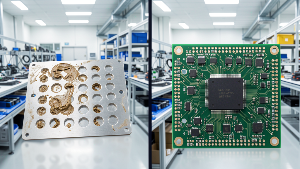
Stencil Cleaning vs. PCBA Cleaning: Different Problems, Different Solutions

Stencil Cleaning vs. PCBA Cleaning: Different Problems, Different Solutions In a standard SMT assembly line, cleaning happens twice — once on the stencil and once on the board. They solve …

Blog / Latest News

Bosch Starts SiC Production in California: Made in America Semiconductor Chips Still Need a Process Ecosystem Behind Them

Last week, Bosch announced it has begun sample production of silicon carbide (SiC) chips at its Roseville, California, factory — the company’s first U.S. semiconductor production facility and a $2 …

Blog / Latest News

Micron’s $250B U.S. Pledge and Section 232 Semiconductor Tariffs: Made in America Still Needs a Process Layer

On July 9, 2026, Micron CEO Sanjay Mehrotra posted on X that Micron is increasing its planned U.S. manufacturing and R&D investment to more than $250 billion through 2035, targeting …

Blog / Latest News

Made in America Means More Than a Facility — It Requires Real Domestic Process Capability

New U.S. facilities for Ultra-HDI PCBs and advanced semiconductor packaging are closing a critical gap in the defense electronics industrial base — but the process ecosystems that make these components reliable still need building.

Blog / Electronic Assembly Cleaning Equipment / Latest News

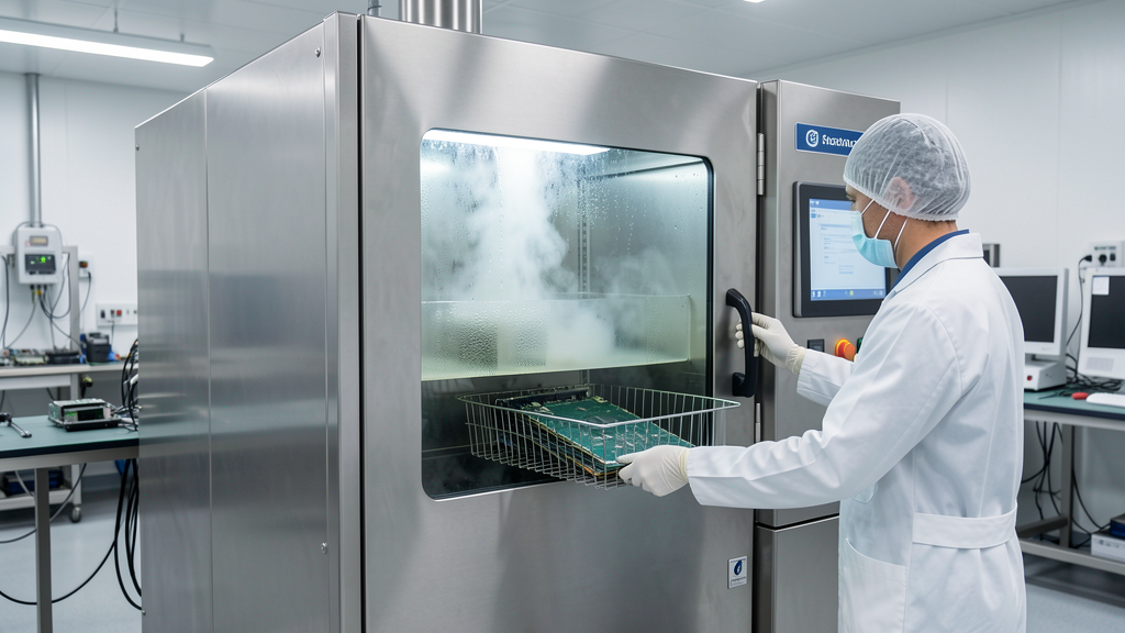
Vapor Degreasing 101: How Closed-Loop Solvent Systems Work

Vapor degreasing has been the gold standard for precision cleaning in electronics manufacturing for decades. Learn how modern closed-loop solvent systems work and why they matter for clean, dry parts in a single operation.

Advanced semiconductor packaging facility - domestic manufacturing process capability
Blog / Latest News

The Advanced Packaging Bottleneck: Why Semiconductor Reshoring Demands More Than Fab Investment

NVIDIA has booked over 50% of TSMC’s advanced packaging through 2027, and 98% of advanced semiconductor packaging is still offshore. What does that mean for defense, aerospace, and medical electronics manufacturers who need domestic process capability beyond the fab?

Domestic semiconductor manufacturing facility - electronics assembly and process equipment
Blog / Latest News

Made in America Is Not a Label — It Is a Process Capability Challenge

Micron begins producing the most advanced memory ever made in America, and NVIDIA pushes domestic manufacturing — but fabs alone don’t close the process capability gap. What defense, aerospace, and medical electronics manufacturers actually need to deliver on the Made in America promise.

Blog / Latest News

Advanced Packaging Is the New U.S. Semiconductor Bottleneck — And Process Capability Is What Closes It

TSMC and Amkor just signed a 10-year deal to build advanced packaging capacity in Arizona. The CHIPS Act is funding fabs across the country. But the real challenge isn’t building …

Blog / Electronic Assembly Cleaning Equipment / Latest News / SMT Cleaning

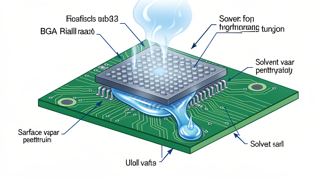
Why Water Can’t Clean Under a BGA: The Surface Tension Problem

Every process engineer who has dealt with flux residue under a low stand-off package has run into the same wall: water doesn’t work. Learn why surface tension prevents water from cleaning under BGAs and why vapor-phase solvent cleaning is the solution.

Blog / Latest News

Made in America Is a Process — Not Just a Label: What the Semiconductor and Defense Electronics Buildout Really Demands

The U.S. is investing billions to bring semiconductor and electronics manufacturing home. But “Made in America” only works if the process capability — cleaning, contamination control, qualification, and reliability — …

Posts navigation

Older posts

About Us

Akrivis Components and Tools supplies specialized process equipment for electronics manufacturing, including cleaning and contamination-control systems, lead forming and cutting equipment, wire bonding, component tinning, and thermal process tools.

Akrivis also represents Purbest Technology Chengdu Co., LTD for the North American market.

Business Hours

Application, quote, and support inquiries are handled during normal business hours. After-hours messages are reviewed the next business day.

  • Monday-Friday: 9am to 5pm
  • Saturday: By appointment
  • Sunday: Closed
  • Vapor SUI Precision Vapor Degreasing System
  • Vapor SUI Mini Vapor Degreasing System
  • Hydro-clean LDS-Plus Cleaning System
  • Automatic Forming Machine APFL
  • Lead Reconditioning System LRS-1
  • Semi-Automatic Bonder PW22
  • Super Tinning Machine
  • Vacuum Heating Plate VTP2000

Company Office

2831 SAINT ROSE PKWY
SUITE 200
HENDERSON, NV 89052
(909) 710-7288
info@akrivistools.com
Copyright © 2026 Akrivis Components and Tools – OnePress theme by FameThemes