
A recent public White House Press Pool post on X framed American manufacturing as a reshoring story, pointing to semiconductors, AI infrastructure, steel, autos and other critical supply chains. For electronics manufacturers, the useful takeaway is not the politics of the headline. It is the operational reality behind it: “Made in America” only becomes meaningful when domestic facilities can run qualified, repeatable processes at production scale.
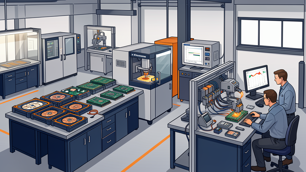
That distinction matters for semiconductor packaging teams, EMS providers, RF and microwave manufacturers, aerospace and defense electronics suppliers, medical electronics manufacturers and federal supply-chain stakeholders. A final product can be assembled in North America, but the constraint is often deeper in the process flow: contamination control, solderability, component preparation, wire bonding, thermal processing, fixture control, inspection, documentation and the ability to support legacy components without losing traceability.
Domestic capacity is moving from policy language to process execution
Several current public signals point in the same direction. NVIDIA says Blackwell chip production has started at TSMC’s Phoenix, Arizona plants, with packaging and test support planned through Arizona partners and AI supercomputer manufacturing planned in Texas. Apple’s American Manufacturing Program expansion includes U.S.-based work with suppliers tied to sensors, integrated circuits, mixed-signal process technologies and semiconductor materials. NIST’s CHIPS for America materials and equipment opportunity remains focused on commercial facilities for semiconductor materials and manufacturing equipment, while its CHIPS R&D BAA supports research, prototyping and commercialization for U.S. microelectronics capability.
Those announcements are not interchangeable, and each has its own scope and legal limitations. But together they reinforce a practical point: domestic electronics resilience is not achieved by changing a label on a purchase order. It depends on whether the factory floor can perform the process steps that make high-reliability electronics manufacturable, inspectable and repeatable.
Where the bottlenecks show up for manufacturers
When semiconductor and electronics work is reshored or expanded in North America, engineering teams often face constraints that are less visible than facility announcements:
- Cleaning and contamination control: flux residues, particulates, ionic contamination, oils and handling residues can turn into yield loss, corrosion risk or latent field failures, especially in high-reliability assemblies.
- PCB, SMT and microassembly cleaning: vapor degreasing, hydro-cleaning and controlled DI-water processes must be matched to materials, package sensitivity, throughput and validation requirements.
- Lead forming, cutting and legacy component preparation: domestic builds often include long-life aerospace, defense, RF, medical or industrial programs where component geometry, standoff, forming stress and reconditioning discipline matter.
- Component tinning and solderability: older or alternate-sourced components may require controlled tinning, oxide removal or solderability support before they can be qualified into production.
- Wire bonding and microelectronics packaging: bond quality depends on surface condition, tool selection, process window, operator skill and documentation — not simply the presence of a bonder.
- Thermal and vacuum process control: heating plates, vacuum systems and controlled thermal processes support drying, curing, preparation and process repeatability across sensitive electronics workflows.
- Traceability and qualification: domestic capacity must stand up to customer audits, program documentation, lot control, rework limits, EHS review and long-term support expectations.
This is why the Made-in-America discussion is highly relevant to process engineers. Domestic fabs, packaging plants, EMS lines and defense electronics programs need more than capacity announcements. They need equipment, tooling and application support that help turn capacity into qualified output.
How Akrivis fits the capability conversation
Akrivis does not claim that every product it represents is Made in USA, Buy American compliant or federally compliant. Those determinations are legal and procurement-specific and must be verified for each program. Akrivis’s role is different: supporting U.S. and North American manufacturers that are building or improving domestic electronics process capability.
That support can include application review and sourcing assistance for cleaning and contamination-control systems, PCB/SMT and microassembly cleaning, vapor degreasing, lead forming and cutting, legacy component reconditioning, wire bonding, component tinning and solderability work, and thermal or vacuum process equipment. For manufacturers under reshoring, CHIPS, defense/aerospace, medical, RF/microwave or federal supply-chain pressure, those process areas can determine whether a domestic program is truly production-ready.
If your team is evaluating a domestic electronics manufacturing process, component-preparation bottleneck, cleaning validation issue, wire-bonding requirement or solderability/reconditioning challenge, contact Akrivis for an application review. The goal is not a patriotic slogan; it is a practical review of the process capability needed to manufacture reliably in North America.
Sources
- White House Press Pool post on X: American manufacturing and reshoring claims
- NVIDIA: American-made AI supercomputers and U.S. manufacturing plans
- Apple: American Manufacturing Program expansion
- NIST/CHIPS for America: semiconductor materials and manufacturing equipment facilities opportunity
- NIST/CHIPS for America: CHIPS R&D Broad Agency Announcement